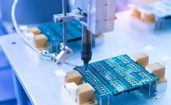
A team of researchers led by the U.S. Department of Energy’s Lawrence Berkeley National Laboratory (Berkeley Lab) developed a powerful new approach that enabled them to directly observe how electrons interact with defects in advanced semiconductor devices with an unprecedented level of detail.